CAN Resistor Emulator Card
Description of the eight channel CAN Resistor Emulator Card HIL Connect hardware
Card Introduction
The CAN Resistor Emulator card is designed to offer PT1000 or NTC resistor emulation capability (also known as thermistor emulation in BMS applications). It relies on a discrete resistor array that achieves the desired resistance by toggling individual resistors through low-resistance relays.
CAN Resistor Emulator card revisions
| Code | Revision | Part number |
|---|---|---|
| LX | 1.2 | 24642 |
| LQ | 1.1 | 24504 |
| LI | 1.0 | 24174 |
Hardware Specification
| Parameter | Value |
|---|---|
| Type | Resistor emulator |
| Number of channels | 8 |
| Input signal range | CAN message |
| Output range | 0..655350 Ω |
| Resolution | 10 Ω |
| Accuracy | ±0.1% ±1.2 Ω |
| Isolation | 200 V |
| Update rate | 5 ms |
| Maximum Power | 0.25 W |
| Comment | Isolation: Channel to chassis |
Hardware Settings
Control of the resistance is done via CAN interface. CAN ID: 0x0 to 0xF is selectable by a rotary switch on the card.
| Option | Method | Possible options |
|---|---|---|
| CAN ID selection | Via internal or external rotary switch | CAN ID set from 0 to 15 |
CAN Message Layout
In a single CAN Message, two resistor channels can be updated. The list of resistor channels is described in Table 4 with definitions below. An example CAN message is provided in the CAN message example section.
| Byte | Message | Start Bit | Stop Bit | Comment |
|---|---|---|---|---|
| 1 | Resistor ID | 1 | 8 | Resistor ID (1,3,5,7) |
| 2 | Resistance MSB | 9 | 16 | Most Significant Byte of 16-bit resistance representation |
| 3 | Resistance LSB | 17 | 24 | Least Significant Byte of 16-bit resistance representation |
| 4 | Resistor ID | 25 | 32 | Resistor ID (2,4,6,8) |
| 5 | Resistance MSB | 33 | 40 | Most Significant Byte of 16-bit resistance representation |
| 6 | Resistance LSB | 41 | 48 | Least Significant Byte of 16-bit resistance representation |
Resistor IDs are ordinal numbers of resistance channels.
Byte 1 can take odd values from 1 to 7.
Byte 4 can take even values from 2 to 8.
Byte 2 is the Most significant Byte of the resistance 16-bit value of the resistor with ID1.
Byte 3 is the Least significant Byte of the resistance 16-bit value of the resistor with ID1.
Byte 2 is the Most significant Byte of the resistance 16-bit value of the resistor with ID2.
Byte 2 is the Least significant Byte of the resistance 16-bit value of the resistor with ID2.
The method for calculating the 16-bit value is the following:
is a binary representation of the resistance value that should be send as a 16-bit message to the resistor emulator. This value takes a range from 0x0000 to 0xFFFF.
is the actual value of the resistance which we want to emulate. Note that it will be rounded to an integer multiple of the value.
is the least significant bit in the binary weighted network of the resistors soldered to the emulation card. For this card, this is 10 Ω.
Channels to be set: 3 and 4 with values 156559 Ω and 10000 Ω respectively
| Byte | 1 | 2 | 3 | 4 | 5 | 6 |
|---|---|---|---|---|---|---|
| Message | RES1 | MSB1 | LSB1 | RES2 | MSB2 | LSB2 |
| Data | 0X03 | 0X03D | 0X28 | 0X04 | 0X03 | 0XE8 |
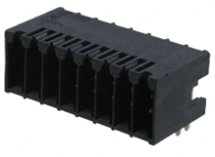
Connector Data
| Type | Mating part |
|---|---|
|
|

Pinout
| Connector | Pin | Resistor channel | Comment |
|---|---|---|---|
| X1 | 1, 2, 9, 10 | R1_1 | Terminal 1 of resistor 1 |
| X1 | 3, 4, 11, 12 | R1_2 | Terminal 2 of resistor 1 |
| X1 | 5, 6, 13, 14 | R2_1 | Terminal 1 of resistor 2 |
| X1 | 7, 8, 15, 16 | R2_2 | Terminal 2 of resistor 2 |
| X2 | 1, 2, 9, 10 | R3_1 | |
| X2 | 3, 4, 11, 12 | R3_2 | |
| X2 | 5, 6, 13, 14 | R4_1 | |
| X2 | 7, 8, 15, 16 | R4_2 | |
| X3 | 1, 2, 9, 10 | R5_1 | |
| X3 | 3, 4, 11, 12 | R5_2 | |
| X3 | 5, 6, 13, 14 | R6_1 | |
| X3 | 7, 8, 15, 16 | R6_2 | |
| X4 | 1, 2, 9, 10 | R7_1 | |
| X4 | 3, 4, 11, 12 | R7_2 | |
| X4 | 5, 6, 13, 14 | R8_1 | |
| X4 | 7, 8, 15, 16 | R8_2 |