Sample rates and timing details for HIL604
devices
IO Timing Details
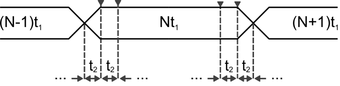
All analog IOs are updated/sampled at the beginning of each simulation time step
(t1), which is software defined. To improve the PWM sampling
resolution, digital inputs actually are sampled at a higher rate (t2),
independent of the simulation time step value. Similarly, digital outputs are
updated at a higher t2 rate. For overall expected loop-back latency,
please consult Loopback Latency.
Figure 1. IO timing diagram
Table 1. Key Timing Parameters
Symbol
Parameter
Value
t1
Simulation step
Software defined
t2
Digital input sampling time
160 MSPS
Table 2. HIL604 IO sample/update rates
IO class
Sample/Update rate
Comment
Digital input
160 MSPS
All digital inputs are sampled simultaneously.
Digital output
Up to 160 MSPS
All digital outputs are updated simultaneously.
Analog input
1/t1
All analog inputs are sampled simultaneously. Minimum sample time
is 1μs