
Solid State Transformer
This demonstration presents a Controller Hardware-in-the-Loop (C-HIL) simulation of a Solid-State Transformer (SST).
Introduction
Solid State Transformers (SSTs) are emerging as a key technology for future smart grid systems. Unlike conventional bulky copper-and-iron transformers, SSTs act as intelligent interfaces capable of active power management, voltage regulation, reactive power compensation, and fault isolation. This application note presents a Controller Hardware-in-the-Loop (C-HIL) demonstration of a 100-kVA SST topology, originally proposed to interface a 7.2 kV AC distribution grid with a 1 kV DC bus.
Model description
This demonstration presents a Controller Hardware-in-the-Loop (C-HIL) simulation of a Solid-State Transformer (SST). The simulated SST topology, shown in Figure 1, is divided into two subsystems: a three-module Cascaded H-Bridge (CHB) functioning as the Active Front End (AFE), followed by a Dual Active Bridge converter on each CHB module. The outputs of the three DAB modules are connected in parallel to supply the final DC load. The system's control architecture is distributed across two separate Texas Instruments LAUNCHXL-F28379D microcontrollers, which are connected to the HIL606 using the HIL TI uGrid Launchpad Interface:
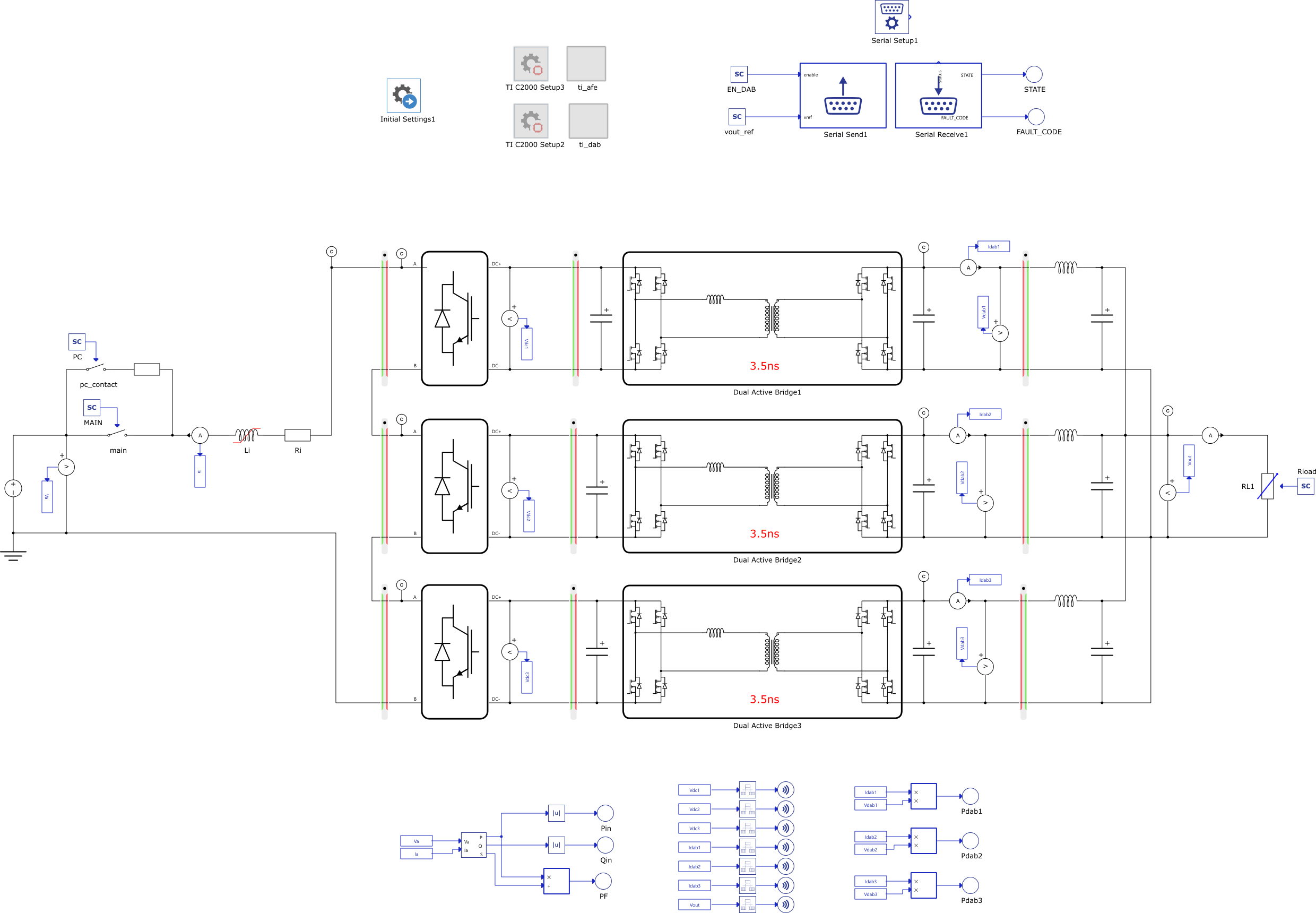
Active Front End (AFE):The AFE is connected to the grid through a simple L-filter. The first controller manages this entire AFE subsystem. Its primary functions are to guarantee a 4 kV voltage balance at the output of each CHB module and to maintain a unity power factor at the grid input.
Dual Active Bridge (DAB) Converters:The second controller regulates the final parallel output voltage to a desired SCADA-controlled setpoint (1 kV by default). It also ensures that equal power is drawn from each of the three CHB modules. This power balance is achieved by actively controlling the output power of each individual DAB module. At its output, a low-pass filter is integrated to ensure a smooth output voltage and current. The DAB operates at a switching frequency of 100 kHz, and its control loop is updated at 20 kHz.
All values of passive elements can be found in the model initialization panel.
AFE Control System
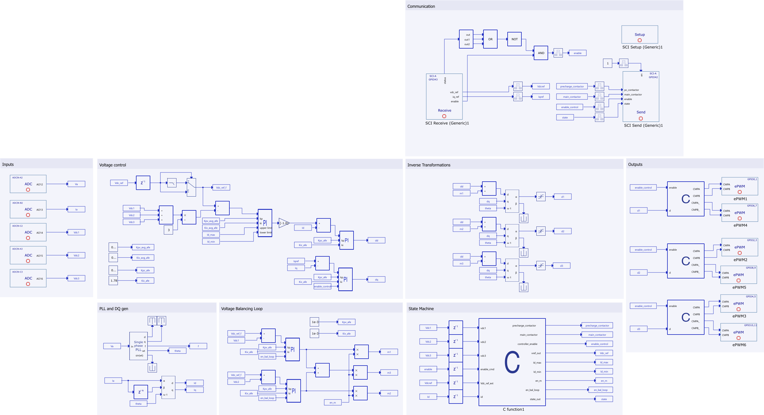
The AFE control architecture employs a single-phase dq vector control strategy. To apply the dq transformation to a single-phase system, an imaginary orthogonal phase is generated, delayed by 90° from the original grid voltage. The control structure consists of the following cascaded loops:
Outer Voltage Loop: This loop is responsible for regulating the average output voltage. The reference DC voltage is compared to the average of the three CHB module voltages. This comparison generates the active d-axis current reference through a proportional-integral (PI) controller.
Inner Current Loop: This loop is responsible for regulating the Id and Iq currents. The active current reference is generated by the outer voltage loop. The reactive q current reference (Iqref) is set to zero by default, ensuring the system maintains a unity power factor at the grid input. The loop regulates the grid current to track these references through identical PI controllers, outputting a common active duty cycle (dd) and reactive duty cycle (dq).
Voltage Balance Loop: To mitigate inherent cascaded unbalances, the voltages of the first two modules (Vdc1 and Vdc2) are individually compared to the reference voltage. This generates compensation duty cycle values (m1 and m2) that are added to the common dd value generated by the inner d-current loop for each module. For the third module, the compensation added is the negated sum of the first two modules. This ensures the total active power drawn from the grid remains unchanged.
Each module computes its inverse dq-axis transformation using its individually corrected active duty cycle (dd + m) and the common reactive duty cycle (dq). The CHB utilizes Phase-Shifted modulation, in which all carrier waves range between 0 and 1 and are shifted by 120 degrees (360 degrees divided by the number of modules).
To ensure proper start-up sequencing and system management, the AFE controller incorporates a state machine. The detailed transitional logic and operational states are implemented within a dedicated C function block in the simulation model.
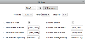
The model sends the enable start up, Vdc reference and Iq current reference through a serial communication using USB between the SCADA and the Controller. On the other hand, the controller sends the precharge, main contactor signals and current state for control and visualization purposes.
When opening the SCADA Panel, do not forget to connect to the write COM port so the serial communication can start.
DABs Control System
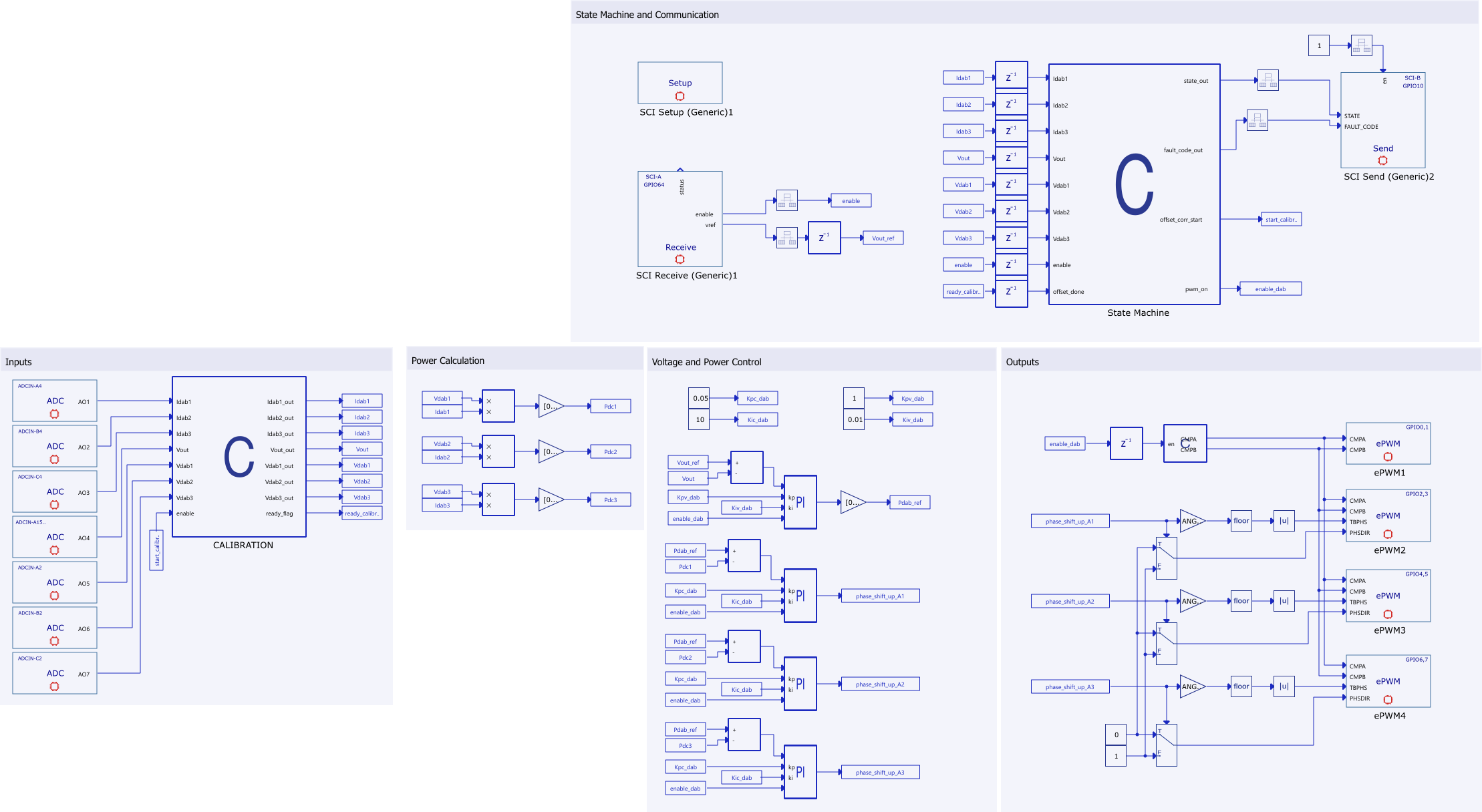
The DAB control architecture is designed to regulate the final parallel DC output voltage while ensuring equal power extraction from each of the three Active Front End (AFE) modules. This active power balancing is critical to maintaining the stability of the intermediate DC links. The control structure consists of the following cascaded loops:
Outer Voltage Loop:This loop is responsible for regulating the common output voltage. The measured parallel output DC voltage is compared to the SCADA-controlled reference (1 kV by default). This error is processed by a proportional-integral (PI) controller to generate a total active power reference required by the load.
Power Balance Loop:This loop ensures that the total power demand is distributed equally among the three DAB modules. The total power reference is divided by three to generate individual power references for each module. These references are compared to the actual power processed by each module, and individual PI controllers generate the required phase-shift angles. Note that the calculated output powers are scaled by a factor of 10000 so the control system works with smaller and more precise numbers.
Each DAB module utilizes Single-Phase Shift modulation. The controllers output the respective phase-shift angle between the primary and secondary full-bridge converters of the high-frequency transformer to dictate the direction and magnitude of power flow. The DAB converters operate at a switching frequency of 100 kHz, with the digital control loop updating at 20 kHz. A low-pass filter is integrated at the output stage to ensure the final DC voltage and current remain smooth and free of high-frequency ripple.
The model receives the Vdc reference and enable signal through a serial communication using directly a digital pin of the HIL set up on the Schematic. Besides that, the controller sends the current state for control and visualization purposes.
Simulation
This application comes with a pre-built SCADA panel (Figure 5). The panel offers the most essential user interface elements (widgets) to monitor and interact with the simulation in real time. Feel free to customize it to fit your needs.
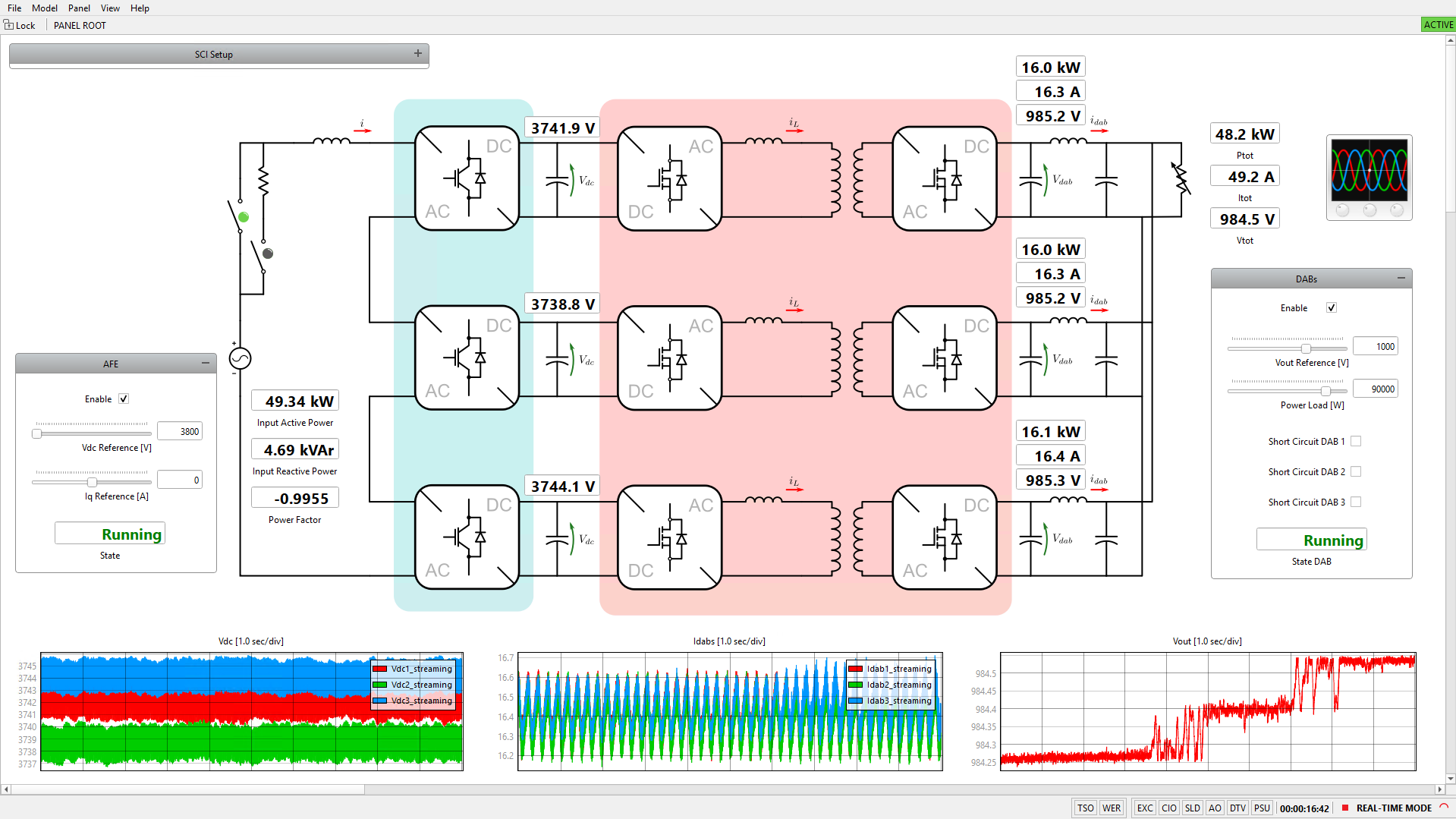
The system can be started up by clicking the ENABLE button of the AFE subsystem. The DC bus voltages will now increase until they reach the reference value. Note that while the second stage is not active, the voltages on the DC bus will vary, since the voltage balancing system is not effective under no-load conditions.
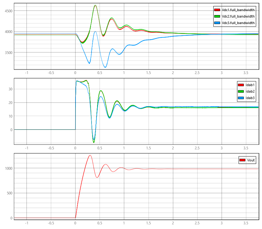
Before starting the DAB stage, open the Capture/Scope Widget and select the Capture mode using the ‘Steps’ preset (located in the top-right corner). The trigger is already set to a change on the output DC voltage's rising edge. Now, press the ENABLE button of the DAB stage, and the scope will be triggered. The response is shown in Figure 6. Note that as soon as the output stage is started under load, Vdc1, Vdc2, and Vdc3 begin to be balanced by the AFE. The output voltage reaches its default value of 1 kV.
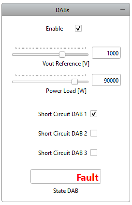
One unique feature of Typhoon DAB implementation is the Short Circuiting one leg test while keeping stable simulation. This event can be triggered by checking any of the Check Buttons ‘Short Circuit DAB’ and the corresponding, as shown in Figure 7
In addition to these tests, the Vdc reference voltage can be changed, and additional output load steps can be applied. While not shown here, it is highly encouraged to further investigate these dynamics in the model by modifying the proportional-integral (PI) controller gains and physical plant parameters. Adjusting these values provides a deeper understanding of the system's stability margins and allows analyzing how the dynamic response behaves under varying operating conditions and setpoint changes.
Test automation
We don’t have a test automation for this example yet. Let us know if you wish to contribute and we will gladly have you signed on the application note!
Example requirements
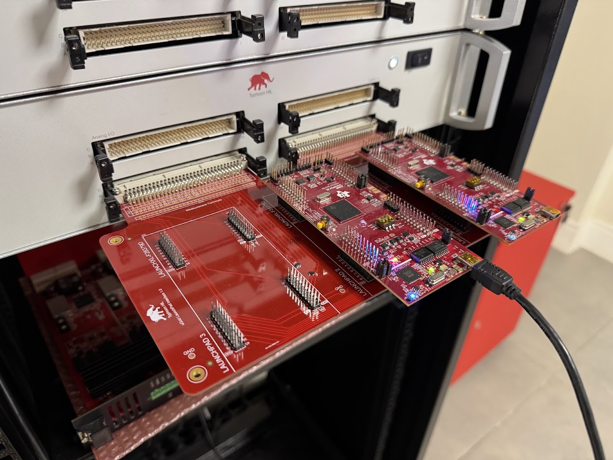
The microcontrollers interface with the Typhoon HIL simulator via the HIL TI uGrid Launchpad Interface: The DAB controller must be connected to Position 1 on the interface board; The AFE controller must be connected to Position 2 on the interface board (keep USB connected between this controller and PC).
To flash the firmware onto the control system, the following steps must be performed for one controller at a time:
Connect the USB cable to the target controller.
In the HIL software, uncomment the corresponding control block and TI settings.
Navigate to the Build and Deploy menu.
If the code does not deploy automatically, click Flash target.
Once the firmware is successfully flashed to both boards, the control logic becomes self-starting upon power-on, and continuous PC-to-controller communication is no longer required. All real-time commands, feedback signals, and SCADA setpoints are managed entirely via the interface board’s analog and digital I/O. In this standalone state, the USB cables serve only as a power supply and can be completely removed if the controllers are configured to draw power directly from the HIL TI uGrid Launchpad Interface.
Table 1 provides detailed information about the file locations and hardware requirements for running the model in real-time, followed by the HIL device resource utilization when running the model using this minimal hardware configuration. This information is provided to help you with running and customizing the model as you see fit.
| Files | |
|---|---|
| Typhoon HIL files | Available by request, please contact us. |
| Minimum hardware requirements | |
| No. of HIL devices | 1 |
| HIL device model | HIL606 |
| HILCore configuration | Custom, please contact us for more information. |
| Interface | 2x Texas Instruments LaunchPad XL TMS320F28379D (DAB Controller under test and AFE) |
| HIL device resource utilization | |
| No. of processing cores | 4 |
| Max. matrix memory utilization | 2.69% (core3) 2.56% (core2) 44.04% (core1) 2.69% (core0) |
| Max. time slot utilization |
46.43% (core3) 91.43% (core2) 48.57% (core1) 40.71% (core0) |
| Simulation step, electrical | 0.5 µs |
| Execution rate, signal processing | 100 µs |
Authors
[1] Nicolas Baschera